Microsoft and Atomico are backing a Norwegian startup replacing light with helium atoms. If it works, this isn’t an upgrade — it’s the end of the photon era in chip manufacturing.
Lace Lithography, a Norwegian deep-tech startup building atom-based semiconductor manufacturing systems, has raised $40 million in Series A funding, signaling a potential shift beyond ASML’s EUV dominance and toward a fundamentally new paradigm: patterning chips with atoms instead of light.
The bet is simple — and radical. The semiconductor industry has spent decades assuming photons could keep shrinking transistors indefinitely. That assumption is now breaking.
ASML’s latest High-NA EUV machines cost more than €700 million per unit, while power consumption per fab is approaching grid scale. At the same time, the diffraction limit — the physical boundary of light itself — is no longer theoretical. It is an engineering constraint the industry is actively running into.
Lace is not trying to push that boundary further. It is stepping around it.
The Physics Was Never the Bottleneck
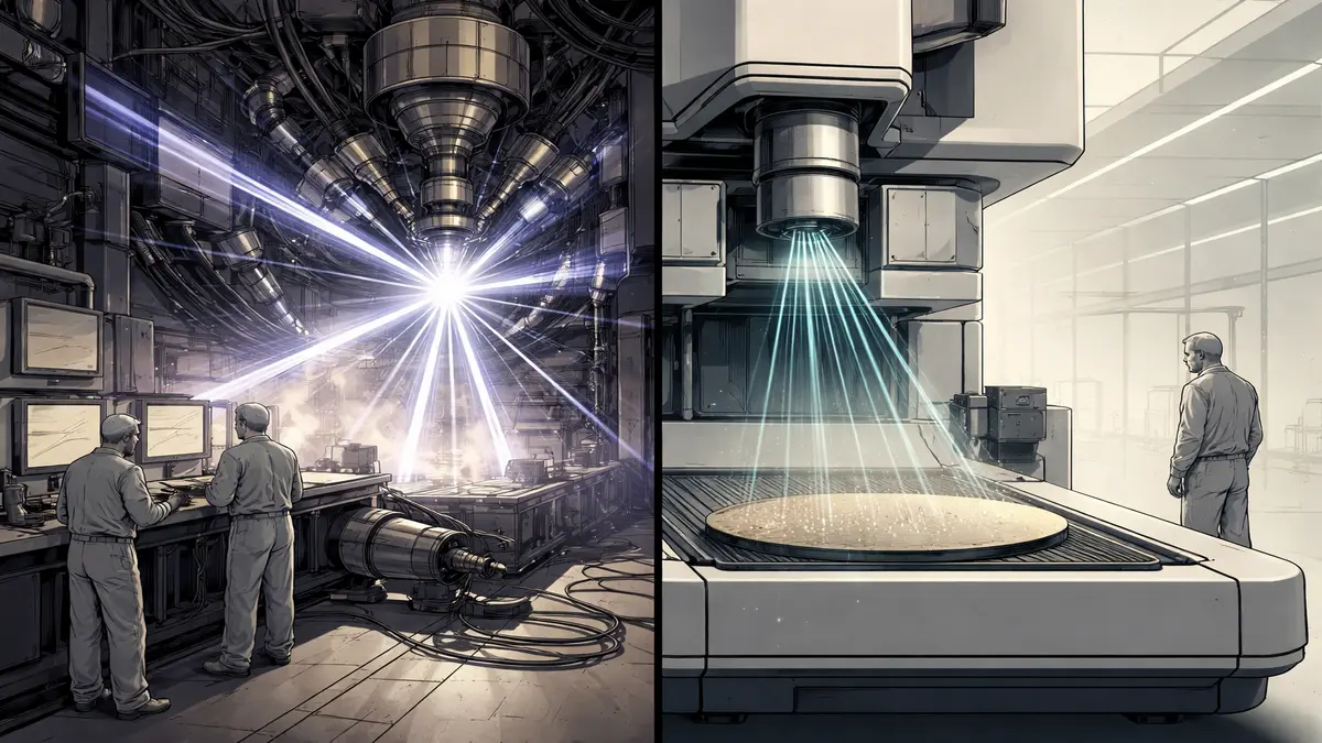
The core idea behind Lace is not new. Metastable helium atoms carry an effective wavelength of roughly 0.1 nanometers — an order of magnitude smaller than EUV systems can resolve today. In theory, this enables significantly higher transistor density and opens a path beyond current scaling limits.
Researchers at Imec have described the potential resolution as “almost unimaginable,” reflecting just how far atom-based lithography could extend miniaturization.
But the real bottleneck was never the beam. It was the mask.
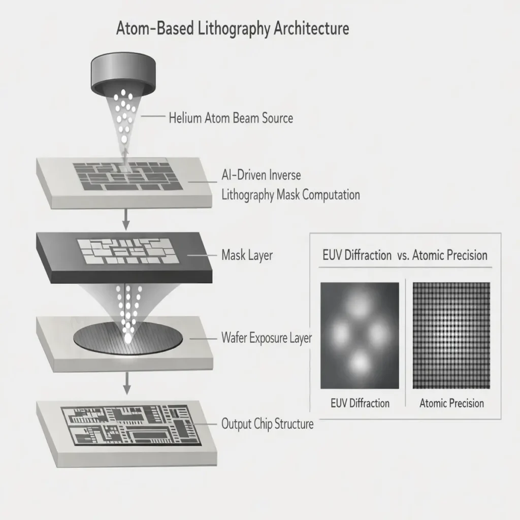
Designing masks for atom-beam lithography required solving an inverse problem so complex it was long considered computationally intractable. Lace’s AI-driven inverse lithography system reportedly delivers a 15-order-of-magnitude speedup, effectively removing the barrier that kept atom-beam systems confined to research environments.
The physics belongs to nature. The algorithm belongs to Lace.
Why Microsoft Is Paying Attention
Microsoft’s participation through its M12 venture arm is the signal that matters most. The company operates one of the world’s largest AI compute infrastructures and is directly exposed to the limits of current semiconductor manufacturing.
Today, ASML controls roughly 90% of leading-edge lithography. That concentration creates a single point of failure in the global AI hardware supply chain — one that hyperscalers, governments, and foundries are all increasingly aware of.
Microsoft’s position in Lace is not simply a financial investment. It is a strategic hedge against that dependency, and a bet that the next generation of compute infrastructure will require a fundamentally different manufacturing approach.
This aligns with a broader shift across AI systems, where control layers are replacing traditional monitoring systems, execution-layer AI is automating real-world workflows, and AI infrastructure control planes are redefining how systems operate.
Lace represents that shift reaching the physical layer of compute itself.
The Real Competitive Landscape
The race beyond EUV is already underway, but not all approaches are equivalent.
Substrate is pursuing particle-accelerator-based X-ray lithography, with ambitious resolution targets but open questions around manufacturability. xLight is working on a free electron laser EUV source, representing an incremental improvement within the photon-based paradigm. Multibeam, meanwhile, is deploying electron beam systems that are already commercially viable but constrained by scattering effects that limit ultimate resolution.
Lace’s approach is fundamentally different.
Photons are limited by diffraction. Electrons are limited by scattering. Helium atoms are constrained by neither in the same way.
That distinction is not marketing. It is physics.
There are currently no direct competitors commercializing atom-beam lithography at scale. Lace is not entering a crowded market — it is defining a new one.
The Risk Is Not Physics — It Is Manufacturing
The science works. The algorithm works. The challenge now is scale.
Atom-beam systems must overcome several major engineering constraints, including throughput, vacuum system complexity, resist material compatibility, and atomic-level alignment precision. Current EUV systems process hundreds of wafers per hour, while atom-based systems have yet to demonstrate comparable production rates.
Lace’s target of deploying a pilot system by 2029 is ambitious, and success will depend on whether these engineering challenges can be solved within a commercially viable framework.
The nature of the risk, however, has shifted. This is no longer a question of whether the technology is possible. It is a question of whether it can be industrialized.
And in semiconductors, that distinction is decisive.
What This Means for AI Hardware
The economics of semiconductor manufacturing are reaching a breaking point. The cost of leading-edge lithography systems, combined with the infrastructure required to operate them, is concentrating capability in the hands of a small number of companies.
If Lace delivers on even part of its promise, the implications extend beyond lithography.
Higher transistor density, lower energy consumption, and more efficient manufacturing could reset the cost structure of AI hardware. That, in turn, would expand access to advanced compute and reshape the competitive landscape of the entire AI industry.
AI is no longer constrained by software innovation alone. It is constrained by the cost and scalability of the hardware it runs on.
Europe’s Second Bet on the Future
For decades, Europe’s role in semiconductor manufacturing has been defined by ASML. Lace represents a second, more experimental attempt to establish leadership at the frontier of chip production.
With operations across Norway, Spain, the United Kingdom, and the Netherlands, and backing from both venture capital and climate-focused investment funds, the company reflects a broader effort to diversify and strengthen Europe’s position in the semiconductor supply chain.
Whether Lace succeeds or not, the scale of its funding and the credibility of its backers ensure that it will be taken seriously by both industry and policymakers.
The Window That Matters
The next two years will be decisive.
Lace has validated the underlying science, secured capital, and established credibility within the semiconductor ecosystem. What it has not done is deliver a production-ready system.
The 2027–2028 window — when prototype performance data begins to emerge — will determine whether Lace represents a true paradigm shift or another ambitious attempt that fails to bridge the gap between laboratory success and industrial deployment.
For investors, this is the real inflection point. For the broader industry, it is the moment when ASML’s dominance either faces its first credible structural challenge or remains intact.
Editorial Close
The atoms are real. The algorithm works.
What remains is manufacturing.
And in semiconductors, that is where revolutions either scale — or disappear.
This one has crossed the physics barrier. Now it has to cross the harder one.
Research Context
Based on Atomico investment materials, Reuters reporting (March 2026), Lace Lithography disclosures, Imec commentary, EU Nanolace project data, and competitive semiconductor intelligence.
Editorial Note
This article reflects independent analysis of publicly available information and broader semiconductor and AI infrastructure trends. TechFront360 has no commercial relationship with any company referenced.